The covalent connection between 2D materials improves device optoelectronic response
13.01.2025
 |
|
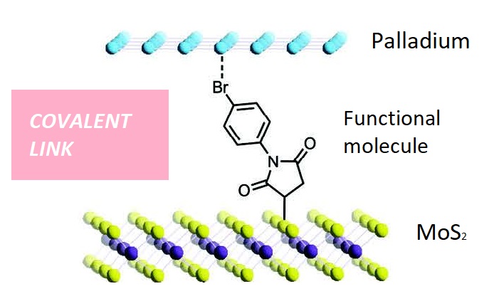
Illustration of a molybdenum disulphide layer attached to a palladium layer via functional molecule. Credit: Ramiro Quirós. |
- Researchers chemically link 2D materials using a molecular ‘velcro’, resulting in a device with improved optoelectronic properties.
- The device, made of palladium nanosheets covalently bonded with MoS2, shows an enhanced optoelectronic response in the infrared.
- The next generation of 2D-2D heterostructures goes beyond van der Waals thanks to the strong covalent bonds between 2D materials.
| Tweet | Suscríbase a las notas de prensa |
Madrid, January 13th, 2025. Combining the best of different crystals to obtain the ultimate material is the motto that drives two-dimensional (2D) materials research. 2D structures are typically built by atomic deposition and weakly bonded to each other by van der Waals interactions. In the last few years, an alternative approach for creating robust 2D structures has been introduced, involving the chemical linkage of nanosheets of distinct materials. Now, researchers are leveraging this technique to create improved devices with a richer optoelectronic response.
In a recent collaboration among IMDEA Nanociencia, INMA-Zaragoza, ICMM and ARAID Foundation, researchers have synthesized and characterised a 2D structure composed of palladium nanosheets and molybdenum disulfide (MoS2). MoS2 is one of the most popular 2D materials because of its facile exfoliation and excellent optoelectronic properties. It features a well-defined bandgap in its 2H type and good absorbance in the visible range of the spectrum. However, a notable limitation of MoS2 is its poor absorbance in the infrared. The broadband optical detection ability, especially from ultraviolet to the near infrared range, is critical for applications including medical monitoring, video imaging or optical communications.
In their latest work, researchers have combined MoS2 with palladium nanosheets to create 2D structures with broadband detection that provide absorbance in the infrared. The prototype device, consisting on a single layer of MoS2 covalently functionalised with palladium nanosheets, showed an enhanced optoelectronic response, both in terms of width and intensity, in comparison with a van der Walls structure with the same components. Researchers proved that the enhancement stemmed from the chemically bonded interface between the two materials. The spectroscopic analysis of the palladium-MoS2 device revealed an electronic interaction between the two materials that evidence the effectiveness of the chemical connection.
The device reported here presents three key features. First, a MoS2 large lateral size in the micrometer range combined with ultrathin thickness of less than 5 nanometres. Second, the palladium nanosheets 2D morphology that enables a strong absorbance in the infrared region. Last, the chemical connection between the two nanomaterials facilitated via a bifunctional molecule.
The work, recently published in Small, highlights the advantages of the covalent connection. First, the device is robust against solvents or thermal processes. Further, the covalent connection between its 2D components improves the device’s optoelectronic response in comparison to its van der Waals counterpart. These findings demonstrate that covalent linked 2D materials hold promise for its application in broad-band photodetection.
This work is the result of a collaboration among Spanish scientists, led by Emilio M. Pérez and Juan Cabanillas at the Madrid Institute for Advanced Studies in Nanoscience (IMDEA Nanociencia), Jesús Santamaría and Victor Sebastián at the Institute of Nanoscience and Materials (INMA-CSIC-UNIZAR), Andres Castellanos-Gomez at the Materials Science Institute of Madrid (ICMM-CSIC) and Raul Arenal at ARAID Foundation, and is partially funded by the accreditation Excellence Severo Ochoa awarded to IMDEA Nanociencia (CEX2020-001039-S).
Reference:
R. Quirós-Ovies, P. Bastante, S. Hettler, V. Vega-Mayoral, S. Aina, V. Balos, T. Pucher, A. Castellanos-Gomez, R. Arenal, J. Cabanillas-Gonzalez, E. M. Pérez, J. Santamaría, V. Sebastian, Chemically-Linked Heterostructures of Palladium Nanosheets and 2H-MoS2. Small 2024, 2406030. https://doi.org/10.1002/smll.202406030
![]() Link to IMDEA Nanociencia repository: https://hdl.handle.net/20.500.12614/3819
Link to IMDEA Nanociencia repository: https://hdl.handle.net/20.500.12614/3819
Contact:
Emilio M. Pérez
Emilio.perez (at)imdea.org
Chemistry of Low Dimensional Materials Group
https://nanociencia.imdea.org/chemistry-of-low-dimensional-materials/home
@emiliomperezlab.bsky.social
Juan Cabanillas
juan.cabanillas (at) imdea.org
Pump-probe Photoinduced Absorption Spectroscopies Group
https://nanociencia.imdea.org/pump-probe-and-photoinduced-absorption-spectroscopies/home
Oficina de Divulgación y Comunicación en IMDEA Nanociencia
divulgacion.nanociencia [at]imdea.org![]()
![]()
![]()
![]()
![]()
Source: IMDEA Nanociencia.
IMDEA Nanociencia Institute is a young interdisciplinary research Centre in Madrid (Spain) dedicated to the exploration of nanoscience and the development of applications of nanotechnology in connection with innovative industries.
Related information:
Beyond van der Waals: next generation of covalent 2D-2D heterostructures https://nanociencia.imdea.org/outreach/press-releases-scientific-advances/item/beyond-van-der-waals-next-generation-of-covalent-2d-2d-heterostructures?category_id=1480


